Chip Gallery
ALL-DIGITAL SUB-GHZ IR-UWB TRANSMITTER BASED ON AN ASYNCHRONOUS LOGIC PLL
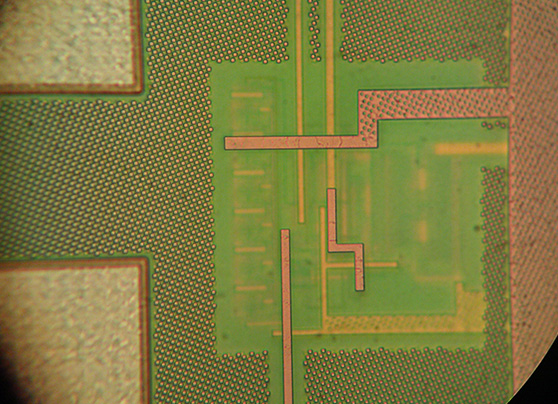
The chip contains an impulse-radio ultrawideband transmitter (TX) based on a ring oscillator capable of synthesizing pulses with both controlled center frequency and bandwidth using a single duty-cycling/trigger reference input. The TX embeds a single-phase charge-pump phase-locked loop (PLL), implemented with asynchronous logic, with 55 logic elements overall. The system, including radio frequency output buffers, consumes measured 30-45 pJ/pulse with a measured efficiency of ~ 47% at 285 MHz center frequency and Vdd in the range of 0.97-1.17 V.
AN ULTRA-LOW POWER PULSED DIGITAL RADIO BASED ON LOGIC CELLS
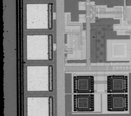
The chip is an ultra-low-power radio receiver implemented only with CMOS logic gates used as basic building blocks and proves its operation. The self-timed duty-cycled system is self-synchronized with the input radio signal, runs a noise-robust baseband detection and does not require any reference besides power supply. Based on S-OOK modulation, the 350-450 MHz digitalradio RX occupies an area of 0.07 mm 2 in a 130 nm RFCMOS technology and achieves a 0.1% sensitivity of -63 dBm at 95 kbps, 380 MHz center frequency and 40 μW active power consumption at 1.1 V power supply. At 1.0 V it achieves -62 dBm sensitivity and 33 μW active power at ~ 0.1% error rate.
ALL-DIGITAL AND ULTRA MINIATURIZED UWB TRANSMITTER
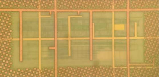
This chip is a very low-complexity all-digital IR-UWB transmitter that can generate pulses in the band 0-5 GHz, requiring a silicon area lower than a PAD for signal I/O. The transmitter, suited to non-standardized low data rate applications, is prototyped in a 130 nm RFCMOS technology and includes analog control signals for frequency and bandwidth tuning. Center frequency is linearly selected with voltage supply, 0.5 V for the range 0-960 MHz and 1.1 V supply for the higher 3.1-5GHz range. The architecture is based on the same delay cell for both baseband and radio frequency signal generation and pulses fractional bandwidth remains constant when voltage supply and control voltages scale. At 420 MHz center frequency, the transmitter achieves 7 pJ/pulse, and for 4 GHzcenter frequency pulses, it achieves 32 pJ/pulse active energy consumption. The OOK/S-OOKtransmitter occupies an area of 0.004 mm2.
ASYNCHRONOUS AND EVENT DRIVEN IR-UWB RECEIVER FOR VERY HIGH SENSITIVITY SHORT DISTANCE ESTIMATION
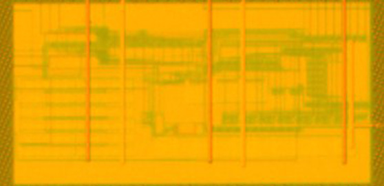
This circuit is a fully asynchronous threshold-based IR-UWB receiver which enables a high sensitivedistance estimation. It includes an ultra-low power baseband unit which achieves 533 fJ/pulse with an asynchronous, multipath robust and time expiring energy detector, which embeds signal strength in the baseband processing latency to increase sensitivity to TX-RX separation. Asynchronous line-of-sight over-the-air measurements obtained with an integrated all-digital transmitter show a maximum sensitivity of 1mm TX-RX separation per nanosecond system latency. The RX also permits data communication based on the use of self-synchronized modulations.
CROC
Small active area (221×79 μm2) capacitive Read-Out Circuit (ROC), robust to supply voltage and temperature variations. The capacitance-to-frequency conversion relies on two ring oscillators, whose frequency ratio is proportional to the capacitance under-test. The system has a resolution of 5.23 fF per LSB, consuming 1.84 μW at Vdd=1.2 V and 1 kHz read-out rate.
Technology
130 nm RFCMOS.
PCROC
Flexible and low power Read-Out Circuit (ROC) with tunable sensitivity (6.7 ÷ 46.4 mbar/LSB), designed to interface a wide range of commercial resistive pressure sensors for robotic applications. The ROC provides contact detection, monitoring small capacitance variations at low pressure (<100 mbar) and encodes pressure measurement on 8 bit, evaluating resistive variations. Two all-digital circuits implement the conversion of the input resistance and capacitance-to-frequency, exploiting an on-chip ring oscillator as timing reference. The active area is 428×159 μm2 and the power consumption is 27.2 μW at Vdd=1.2 V and 1 kHz read-out rate
Technology
130 nm RFCMOS.
M4N2013
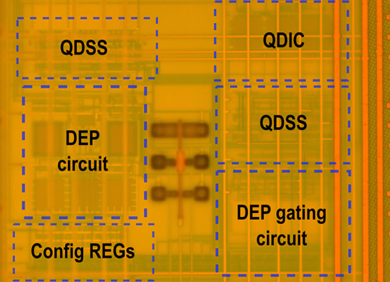
The Micro-for-Nano chip (“nome chip”) has been fabricated in UMC 130nm RFCMOS technology with the aim to integrate an array of nanomaterials on top of silicon chip surface.
This chip includes 8 identical custers named M4N cells. Each one is composed by with 3 Read-Out Circuits (ROCs), a DEP generator and 3 couples of top-electrodes for nanomaterial assembling.
In figure:
– QDIC is a two-quadrant quasi-digital impedance converter which covers a wide input range of resistance (1MΩ – 1GΩ) and capacitance (100fF – 1μF) with SNR>44dB, consumes 14μW and occupies 0.003mm2 on silicon.
– QDSS converter is a quasi-digital single slope resistance converter, based on fully-digital circuits compliant with technology scaling; it is used to read-out resistive materials (10kΩ – 100MΩ), consumes about 50μW and occupies 0.005mm2 on silicon.
– DEP generator is a dielectrophoresis signal generator with adjustable oscillation frequency from 50kHz up to 1MHz
CHIP “MANATEE”
The system is made of eight readout circuits to convert the analog information into a quasi-digital signal. The pulse streams are then temporally ordered to form a single streams of events (arbiter), tagged with a channel and chip address and serialized (encoder), modulated (SOOK modulator), and then wirelessly transmitted (IR-UWB TX).
Technology
UMC 130nm RFCMOS.


